

R&D
The GnK SolutionsR&D lab.
A small, elite team of seasoned engineers that carries out the entire product development cycle in-house.
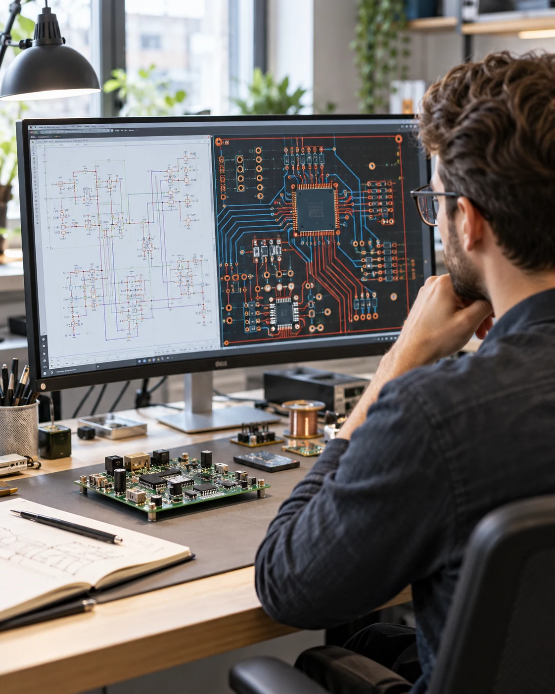
- Specialists in four fields: HW · SW · app · FA
- 10engineers
- Combined hands-on experience of all ten engineers
- 185yrs
- Average experience across the engineering team
- 18.5yrs
- 10+ years in the field: 9 of 10, and 3 with 25+ years
- 90%
Capabilitiesby discipline.
Hardware and software engineers average more than 23 years of experience.
Circuits · boards · design for production
Hardware
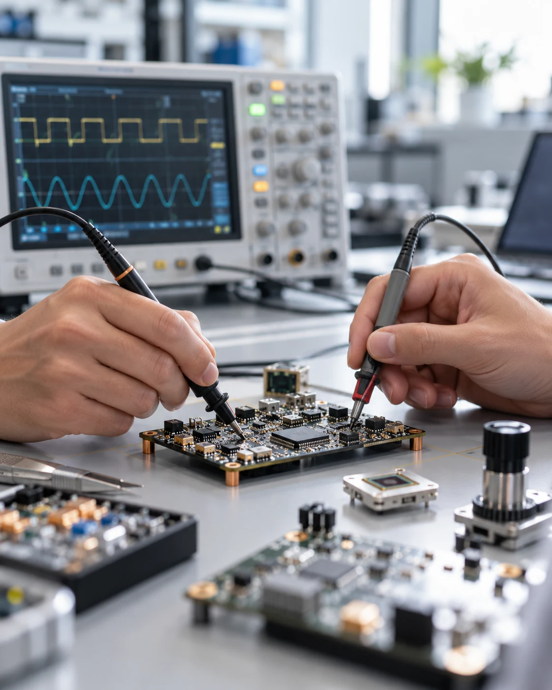
- Team
- 3 engineers
- Experience
- 26.3 yrs avg
- Combined experience
- 79 yrs
- Individual experience
- 35 · 26 · 18 yrs
The whole hardware process in-house, from circuit design and part selection to prototypes and production support.
What we develop and support
Analog4
- Analog circuit design
- Power circuit design
- SMPS · DC-DC converters
- LED drivers
Digital5
- Digital circuit design
- MCU / embedded boards
- Sensor interfaces
- High-speed signals · comms I/F
- Motor drive circuits
RF3
- RF circuit design
- Antenna matching · RF tuning
- EMI / EMC countermeasures
Design · verification4
- Circuit design · PCB ARTWORK (PADS · OrCAD · Altium Designer)
- Circuit simulation / SI / PI simulation (Advanced Design Systems)
- Explosion-proof · high-reliability design
- Part selection · BOM management
Firmware · embedded · communications
Software
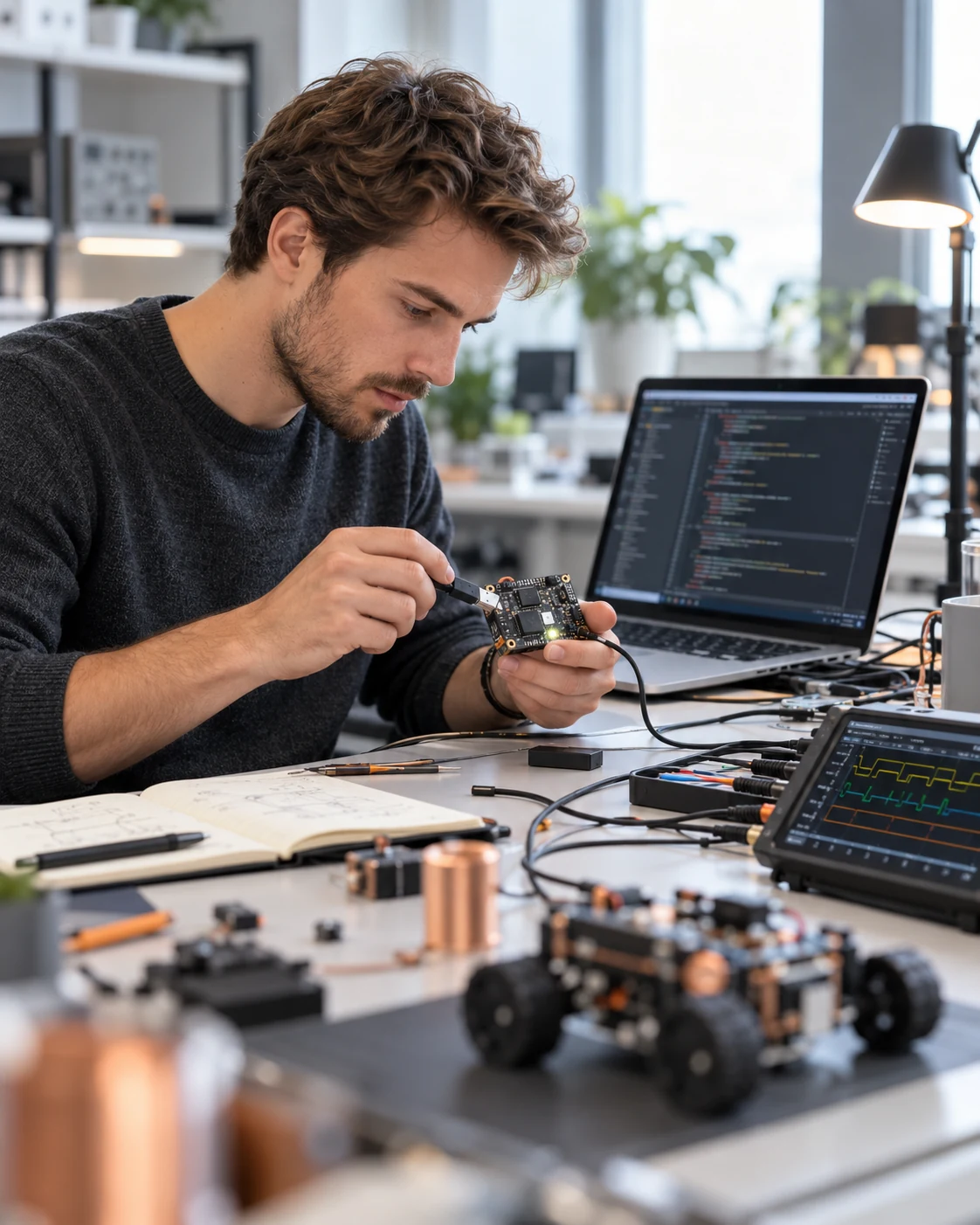
- Team
- 3 engineers
- Experience
- 21 yrs avg
- Combined experience
- 63 yrs
- Individual experience
- 35 · 18 · 10 yrs
Firmware and control software designed with a deep understanding of the hardware, optimizing hardware and software together.
What we develop and support
Firmware · platforms6
- MCU firmware
- RTOS development
- Embedded Linux
- Device drivers
- Bootloaders · FOTA
- Low-power software
Communication6
- UART · I2C · SPI · CAN
- RS-485 · Modbus
- BLE · Wi-Fi
- LoRa · Zigbee
- IoT cloud (MQTT)
- Secure communication · encryption
Control · signal processing2
- Control algorithms (PID and more)
- Sensor signal processing · filtering
Production · test2
- PC test and inspection programs
- Production jig firmware
Mobile · PC · web
Apps
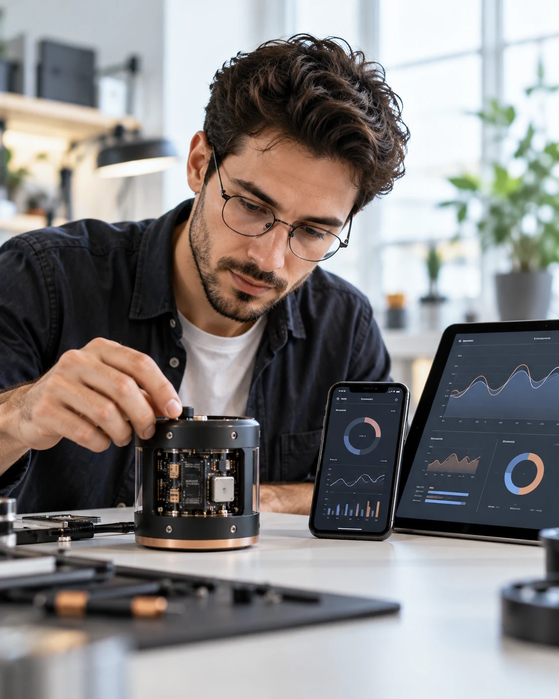
- Team
- 2 engineers
- Experience
- 10 yrs avg
- Combined experience
- 20 yrs
- Individual experience
- 10 · 10 yrs
User applications and UIs that monitor and control equipment and systems.
What we develop and support
Mobile apps5
- Android apps
- iOS apps
- Cross-platform apps
- BLE · Wi-Fi device apps
- Device OTA update apps
PC · web4
- PC applications (C#)
- Web monitoring dashboards
- Server · database integration
- Admin pages
Features · data3
- Remote control · push notifications
- Data logging · reports
- Statistics · chart views
Design · operations2
- UI / UX design
- App release · maintenance
Technical support for customers of the semiconductors we supply
Field application
- Team
- 2 engineers
- Experience
- 11.5 yrs avg
- Combined experience
- 23 yrs
- Individual experience
- 18 · 5 yrs
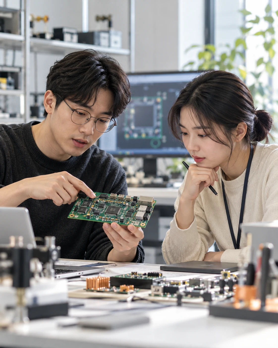
Answering customers' technical questions on the semiconductors we supply, reviewing and fixing circuits, and developing features customers ask for.
See our line cardWhat we develop and support
Technical consulting4
- Chip · MCU technical questions
- Chip selection · alternatives
- Migrating from other vendors' chips
- Customer visits · technical seminars
Design review3
- Schematic review · fixes
- PCB layout review
- Reference designs
Development support5
- Evaluation boards · demos
- Sample firmware · example code
- Custom feature development
- Dev tools · IDE setup
- Flash · memory integration
Production support2
- Production programming
- Failure analysis · troubleshooting
Hardware to app,all in-house.
Hardware and software are developed together, and research, sourcing and manufacturing run as one process — so what ships is finished.
20+ yrs
Hardware design
- ARM7/9/11, Cortex-M3/M4/M7, Cortex-A8/A9/A15
- AC/DC · DC/DC · DC/AC power design
- WiFi · BT · ZigBee RF solutions
- EMC/EMI design for KC · CE · UL
15+ yrs
Software
- Linux · Windows CE · RTOS
- Porting across many operating systems
8+ yrs
Mobile apps
- Android · iOS
- Apps paired with IoT devices
20+ yrs
Mechanical design
- IP54 · IP65 waterproof and dustproof
- 1.2 / 1.5 / 1.8 m drop design
- 3G+ vibration-resistant design
- Pull and twist stress design
Where we've built
- Mobile devices
- Industrial control
- System control
- Medical devices
- Imaging
- Security
- Home · network
- Defense
A board performsthe way it's routed.
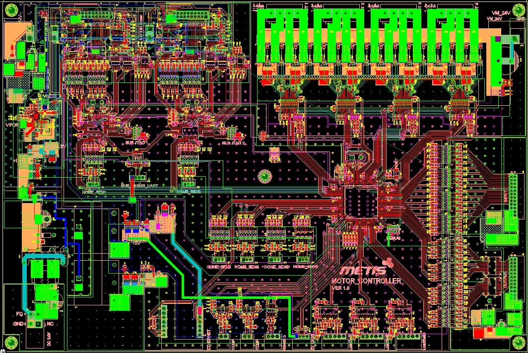
High-speed, RF, analog and power. We design for manufacturability first to cut problems after the prototype — and keep customer data strictly confidential.
Capabilities
- Build-up · full stack-via PCBs
- High-speed boards
- RF boards
- Analog boards
- Impedance-controlled boards
- SI · PI simulation
- EMI · EMC-aware design
- Manufacturability review
Tools
- OrCAD
- PADS Logic
- PADS Layout
- Altium Designer
- CAM350
- AutoCAD
Design process
01Order
Schematics, mechanical drawings, datasheets received
02Spec review
One-pin check, part specs and mechanicals reviewed
03Schematic
OrCAD conversion or new schematic capture
04Part library
In-house common library, new parts registered
05Mapping
Netlist and library checks
06Placement
Mechanical and EMI/EMC review, placement confirmed
07Routing
Impedance and power patterns, parallel work shortens schedules
08Quality check
Automated open/short check, then Gerber delivery
Developedin the GNK lab.
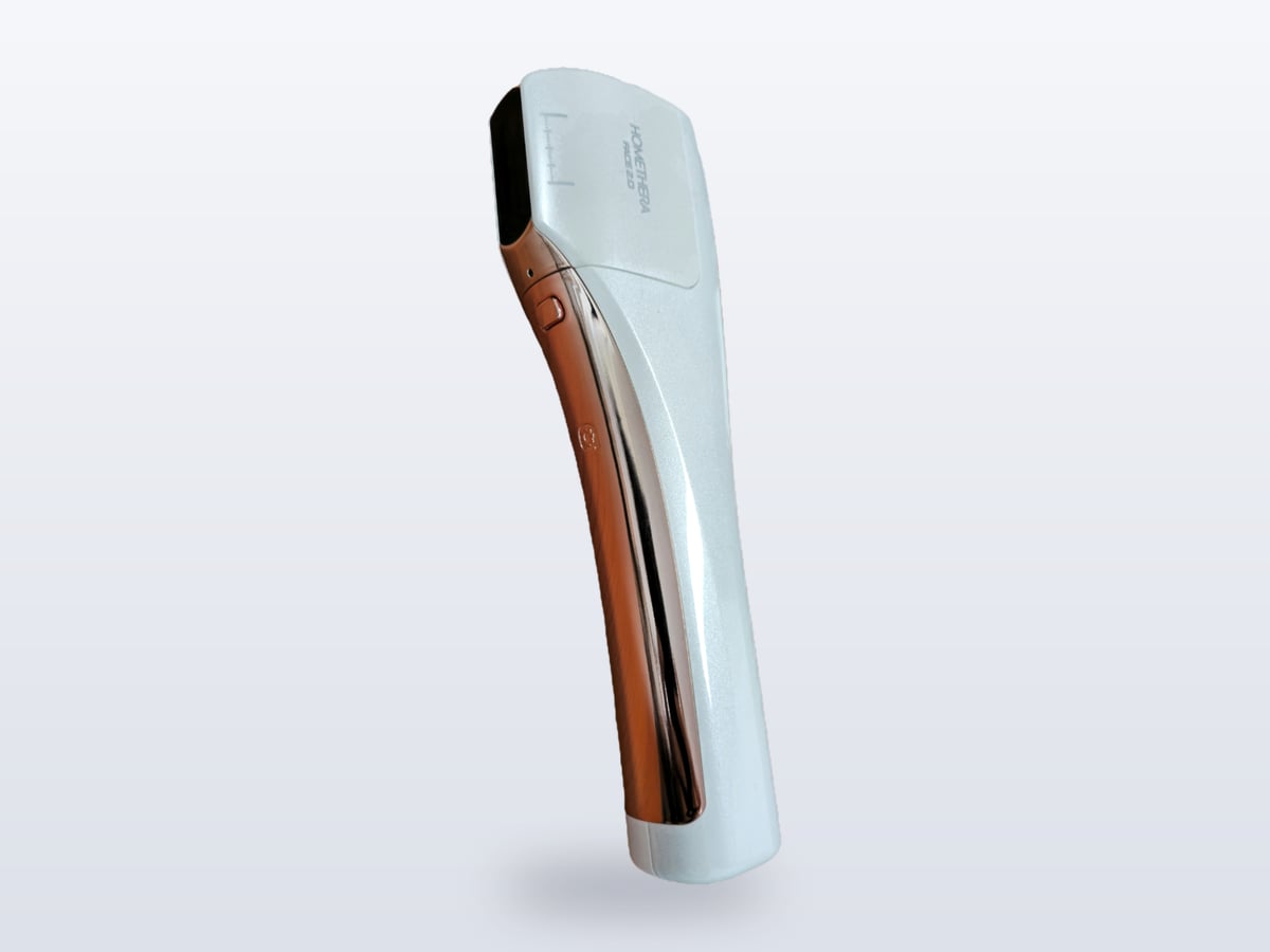
HIFU ultrasonic skin-care device
Homecera-3
A handheld device for skin care using HIFU (high-intensity focused ultrasound) output.
- Output frequency 7.3–7.6 MHz
- Skin penetration depth 2.0 mm / 4.5 mm
- MCU GD32F303RET6 (Arm Cortex-M4)
- Internal battery 11.1 V / 730 mA
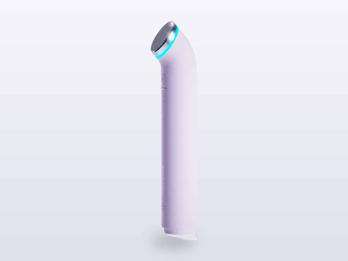
Gentle high-density ultrasonic skin care for home use
LDM (water-drop lifting)
LDM (water-drop lifting): a gentle, high-density ultrasonic skin-care product for home use.
- Output frequency 3 MHz, 10 MHz
- 3 modes: 3 MHz, 3 MHz + 10 MHz, 10 MHz
- 2 levels, output voltage 9 V, 13 V
- Built-in 1-cell 3.7 V 1400 mAh, USB-C charging
Specifications may change without notice as products are improved.
Core strengthsof the lab.
End-to-end
Full-stack in-house development
Everything from hardware, software and app development to customer technical support (FA) is done in-house, without outside help.
18 yrs avg
Proven, senior expertise
Accumulated problem-solving ability and design know-how minimize development risk and trial and error.
Fast
Close collaboration across disciplines
As a small, elite team we decide and give feedback quickly, responding to customer needs fast and flexibly.
35 yrs → 3 yrs
A stable structure for passing on know-how
Experience spread step by step from 35 years down to 3 keeps core technology in-house and builds a base for growth.
From development to delivery, in one company
See manufacturingTell us whatyou're building.
A schematic or a parts list is enough to start. An engineer reviews it and gets back to you personally.